publications, Réseau
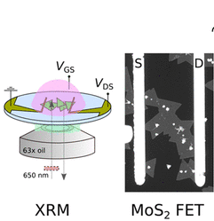
In Operando Study of Charge Modulation in MoS2 Transistors by Excitonic Reflection Microscopy
Monolayers of transition metal dichalcogenides (2D TMDs) experience strong modulation of their optical properties when the charge density is varied. Indeed, the transition from carriers composed mostly of excitons at low electron density to a situation in which trions dominate at high density is accompanied by a significant evolution of both the refractive index and the extinction coefficient. Using optical interference reflection microscopy at the excitonic wavelength, this (n, κ)–q relationship can be exploited to directly image the electron density in operating TMD devices. In this work, we show how this technique, which we call XRM (excitonic reflection microscopy), can be used to study charge distribution in MoS2 field-effect transistors with subsecond throughput, in wide-field mode. Complete maps of the charge distribution in the transistor channel at any drain and gate bias polarization point (VDS, VGS) are obtained, at ∼3 orders of magnitude faster than with scanning probe techniques such as KPFM. We notably show how the advantages of XRM enable real-time mapping of bias-dependent charge inhomogeneities, the study of resistive delays in 2D polycrystalline networks, and the evaluation of the VDS vs VGS competition to control the charge distribution in active devices.
Nathan Ullberg*, Arianna Filoramo, Stéphane Campidelli, and Vincent Derycke*, ACS Nano 2024, 18, 14, 9886–9894
Comments are closed

