publications, Réseau
Field and Thermal Emission Limited Charge Injection in Au–C60–Graphene van der Waals Vertical Heterostructures for Organic Electronics
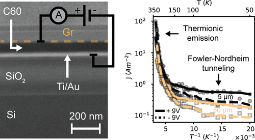
Among the family of 2D materials, graphene is the ideal candidate as top or interlayer electrode for hybrid van der Waals heterostructures made of organic thin films and 2D materials due to its high conductivity and mobility and its inherent ability of forming neat interfaces without diffusing in the adjacent organic layer. Understanding the charge injection mechanism at graphene/organic semiconductor interfaces is therefore crucial to develop organic electronic devices. In particular, Gr/C60 interfaces are promising building blocks for future n-type vertical organic transistors exploiting graphene as tunneling base electrode in a two back-to-back Gr/C60 Schottky diode configuration. This work delves into the charge transport mechanism across Au/C60/Gr vertical heterostructures fabricated on Si/SiO2 using a combination of techniques commonly used in the semiconductor industry, where a resist-free CVD graphene layer functions as a top electrode. Temperature-dependent electrical measurements show that the transport mechanism is injection limited and occurs via Fowler–Nordheim tunneling at low temperature, while it is dominated by a nonideal thermionic emission at room and high temperatures, with energy barriers at room temperature of ca. 0.58 and 0.65 eV at the Gr/C60 and Au/C60 interfaces, respectively. Impedance spectroscopy confirms that the organic semiconductor is depleted, and the energy band diagram results in two electron blocking interfaces. The resulting rectifying nature of the Gr/C60 interface could be exploited in organic hot electron transistors and vertical organic permeable-base transistors.
Jacopo Oswald, Davide Beretta*, Michael Stiefel, Roman Furrer, Sebastian Lohde, Dominique Vuillaume, and Michel Calame, ACS Appl. Nano Mater. 2023, 6, 11, 9444–9452 doi
Comments are closed


